An Scr Has Pn Junctions
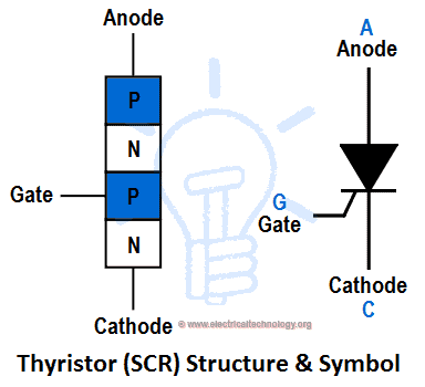
When a pn junction is added to a junction transistor the resulting three pn junctions device is called a silicon controlled rectifier. GTO is 4 layer PNPN device having 3 PN junctions and 3 terminals Gate G Anode A and Cathode C.
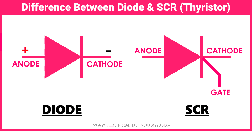
What Is The Difference Between Diode And Scr Thyristor
The wide intrinsic region is in contrast to an ordinary pn diodeThe wide intrinsic region makes the PIN diode an inferior rectifier.
. 1N3716 IN3712 and IN3714 are some of the tunnel diodes. Under such a condition electrons will flow from the semiconductor. An SCR is a three-terminal three-junction and four-layer semiconductor device that is used to perform switching functions in power circuits.
A thyristor is a four-layer solid-state semiconductor device that contains 3 PN junctions in series having 3 terminals called anode cathode and gate. The SCR has three pn junctions and four layer of p and n type semiconductor joined alternatively to get pnpn device. Sometimes the SCR is also called as Thyristor.
In fact SCR Silicon Controlled Rectifier is a trade name given to the thyristor by General Electric Company. Gate terminal as it is the input part taken from MOSFET while the collector and emitter as they are the output taken from the BJT. Therefore the NP junction blocks the flow of a positive current from the anode to cathode.
The layers are either NPNP or PNPN. At BE junction the potential barrier decreases. However unlike the junction diode which is a two layer P-N semiconductor device or the commonly used bipolar transistor which is a three layer P-N-P or N-P-N switching device the Thyristor is a four layer P-N-P-N semiconductor device that contains three PN junctions in series and is represented by the symbol as shown.
The outer layers are heavily dopped and the inner. However their sensitivity is usually very low. It has the ability to control huge current and is generally used.
Cadherins are a class of type-1 transmembrane proteins and they are dependent on calcium Ca 2 ions to function hence their name. Basically SCR is a three-terminal four-layer semiconductor device consisting of alternate layers of p-type and n-type material. The designing of thyristors can be done with 3-PN junctions and 4 layers.
Cadherins named for calcium-dependent adhesion are a type of cell adhesion molecule CAM that is important in the formation of adherens junctions to allow cells to adhere to each other. PNPN and J1 J2 J3. BJT transistor has two PN junctions between its collector and emitter.
It includes three terminals namely anode gate and cathode. Like a diode a thyristor is a unidirectional device as well but unlike diode it can be used as an open circuit switch. The negative resistance is.
FET has either an N-channel or a P-channel between the gate of the P-layer or the N-layer respectively. Hence it has three pn junctions J 1 J 2 and J 3. The Schottky barrier shown in Figure 6-2 is formed by an electron blocking contact for which ϕ m ϕ sThe condition for a contact to be blocking seen by electrons from the metal is ϕ m ϕ s for a metaln-type semiconductor junction or ϕ m ϕ for a metalintrinsic semiconductor or metalinsulator junction.
Working Principle of BJT. Fig1 i It is clear that it is essentially an ordinary rectifier pn and a junction transistor npn combined in one unit to form pnpn device. Cell-cell adhesion is mediated by extracellular cadherin.
Signals and Amplifiers 4 CHAPTER 2 Semiconductors 124 CHAPTER 4 MOS Field-Effect Transistors MOSFETs 230 Bipolar Junction Transistors BJTs 350 Devices and Basic Circuits. SCR usually has three terminals and four layers of alternating p. A thyristor with a P-N-P-N structure has three junctions.
It has three terminals Gate G CollectorC and Emitter E. The channel is used for the flow of majority charge carriers. BJT have two junctions formed by the combination of two back to back PN junctions.
These four-layer form three PN junctions named J1 J2 and J3. In addition to reading the questions and answers on my site I would suggest you to check the following on amazon as well. PN NP and PN.
While in the tunnel diode the concentration of the impurity is about 1 part in 10 3. The figure below shows an SCR with the layers p-n-p-n. All PN-junctions are light sensitive and can be used in a photo-conductive unbiased voltage mode with the PN-junction of the photodiode always Reverse Biased so that only the diodes leakage or dark current can flow.
Base-Emitter junction BE is forward bias while collector-emitter junction CE is reverse bias. The p-type and n-type regions are typically heavily doped because they are used for ohmic contacts. Fig1i shows the construction of an SCR.
The metaloxidesemiconductor field-effect transistor MOSFET MOS-FET or MOS FET is a type of field-effect transistor FET most commonly fabricated by the controlled oxidation of siliconIt has an insulated gate the voltage of which determines the conductivity of the device. The concentration of impurity in the normal PN-junction diode is about 1 part in 10 8. This ability to change conductivity with the amount of applied voltage can be used for.
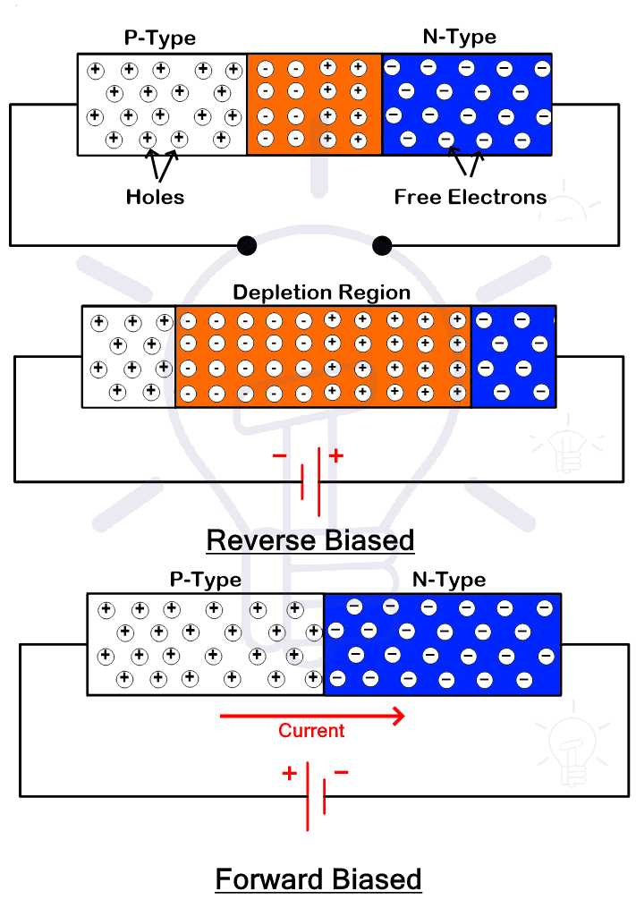
The thyristor or SCR is a power semiconductor device which is used in power electronic circuits. If the anode is a positive terminal with respect to the cathode the outer junctions PN and PN are forward-biased while the center NP junction is reverse-biased. A power diode has a P-I-N structure as compared to the signal diode having a PN junction.
It has a low forward voltage drop and a very fast switching action. One PN junction between Collector and Base and the other between Base and Emitter. Here the I in P-I-N stands for intrinsic semiconductor layer to bear the high-level reverse voltage as compared to the signal diode the n-drift region layer shown in Figure 1.
Schottky also known as Schottky barrier diode or hot-carrier diode is a semiconductor diode formed by the junction of a semiconductor with a metal. GTO aka Gate Turn Off is a semiconductor based fully controlled unidirectional switching device thyristor that has 3 terminals gate cathode and anode. The anode and cathode terminals are placed at the end layers and where the gate terminal is placed with the third layer.
It is a four-layer PNPN device having three PN junctions. They work like a bistable switch and it operates from nonconducting to conducting. This book offers a practical approach with design examples for design engineers and system engineers in the electronics industry as well as the aerospace industry.
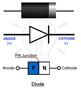
Like the diode the Thyristor is a. A PIN diode is a diode with a wide undoped intrinsic semiconductor region between a p-type semiconductor and an n-type semiconductor region. The terminals name also implies being taken from both transistors.
SCR that can be used as a light activated switch in AC applications. Constructional Details of SCR. SCR has four layers of extrinsic semiconductor materials.
Enter the email address you signed up with and well email you a reset link. The cats-whisker detectors used in the early days of wireless and metal rectifiers used in early. SCR is a four-layered and three junctions unidirectional device ie.
They are also known as PN PN Junction or Latching switches similar to digital latches where it can be used as an ON and OFF switch by controlling its gate input voltage and. Thyristor. The Schottky diode named after the German physicist Walter H.
What Is The Difference Between Diode And Scr Thyristor

What Is The Difference Between Diode And Scr Thyristor
What Is The Difference Between Diode And Scr Thyristor
How Does A Pn Junction Behave As A Capacitor Quora

What Is The Difference Between Diode And Scr Thyristor
What Is The Difference Between Diode And Scr Thyristor
0 Response to "An Scr Has Pn Junctions"
Post a Comment